Day 1 :
Keynote Forum
Carlo Montemagno
University of Alberta, Canada
Keynote: Small things offer big promise
Time : 10:00-10:25

Biography:
Driven by the principles of excellence, honor and responsibility and an unwavering commitment to education as an engine of economic prosperity, Carlo Montemagno, PhD has become a world-renowned expert in nanotechnology and is responsible for creating groundbreaking innovations which solve complex challenges in the areas of informatics, agriculture, chemical refining, transportation, energy, and healthcare. He was Founding Dean of the College of Engineering and Applied Sciences at University of Cincinnati; received a Bachelor of Science degree in Agriculture and Bio Engineering from Cornell University; a Master’s Degree in Petroleum and Natural Gas Engineering from Penn State and a PhD in Civil Engineering and Geological Sciences from Notre Dame. He is now in Alberta as the Director of Ingenuity Lab, professor in the Department of Chemical and Materials Engineering at the University of Alberta, AITF Strategic Chair of Bionanotechnology, Program Lead of the Biomaterials Program at the National Institute for Nanotechnology and Canada Research Chair in Intelligent Nanosystems. “Research and education are critical to success because the transfer of knowledge creates economic prosperity.” — C. Montemagno Carlo Montemagno has been recognized with prestigious awards including the Feynman Prize (for creating single molecule biological motors with nano-scale silicon devices); the Earth Award Grand Prize (for cell-free artificial photosynthesis with over 95% efficiency); the CNBC Business Top 10 Green Innovator award (for Aquaporin Membrane water purification and desalination technology); and named a Bill & Melinda Gates Grand Challenge Winner (for a pH sensing active microcapsule oral vaccine delivery system which increased vaccine stability and demonstrated rapid uptake in the lower GI tract.)
Abstract:
Keynote Forum
Beng S. Ong
Hong Kong Baptist University, Hong Kong
Keynote: Progress in semiconductor materials and processes for printed transistors
Time : 10:25-10:50

Biography:
Beng Ong is presently Director of Research Centre of Excellence for Organic Electronics and Chair Professor of Materials Science at Hong Kong Baptist University. He was formerly a Nanyang Professor at Nanyang Technological University in Singapore, who also held joint appointments as Director at Institute of Materials Research and Engineering and Singapore Institute of Manufacturing Technology. Prior to his relocation to Asia in 2007, Prof. Ong was a Senior Xerox Fellow and 21st-Century Materials Strategist at Xerox Corporation as well as Area Manager at Xerox Research Centre of Canada. Over the years, he had had held adjunct professorships at various universities including McMaster University and University of Waterloo in Canada, and Honorary Professorship at Shanghai East China University of Science and Technology in China. Prof. Ong publishes extensively in advanced materials, organic electronics, nanotechnology, etc. and currently has a patent portfolio of 230 US patents and many foreign equivalent patents.
Abstract:
Keynote Forum
Jas Pal Badyal
Durham University, United Kingdom
Keynote: Scalable functional nanocoatings
Time : 11:05-11:30

Biography:
Jas Pal Badyal FRS was awarded BA/MA and PhD degrees from Cambridge University; where he subsequently held King’s College and Oppenheimer fellowships. He is the primary author / inventor on 175 peer reviewed journal publications / 41 patent families. He has been recipient of the Royal Society of Chemistry Harrison Medal; the British Vacuum Council Burch Prize; the International Association of Advanced Materials Medal; and in 2016 he was elected a Fellow of the Royal Society (FRS) – UK and Commonwealth National Academy of Sciences. His research has led to 3 successful start-up companies: Surface Innovations Ltd; Dow Corning Plasma Ltd; and P2i Ltd.
Abstract:
The worldwide market for functional surfaces exceeds $100 billion per annum (US Department of Energy). A key driver is the added value that can be imparted to commercial products through the molecular engineering of their surface properties. For example, the cleanliness of optical lenses, the feel of fabrics, the resistance of biomedical devices to bacteria, the speed of computer hard disks, and even the wear of car brake pads are all governed by their surface properties. The fabrication of such surfaces requires the incorporation of specific functional groups; for which there exists no shortage of potential methods including: self-assembled monolayers (SAMs), Langmuir-Blodgett films, dip-coating, grafting, chemical vapour deposition, to name just a few. However such techniques suffer from drawbacks including substrate-specificity (cannot be easily adapted to different materials or geometries) and environmental concerns associated with the utilization of solvents, strong acid / base media, or heat. A range of innovative solutions will be described for the molecular tailoring of solid surfaces. Applications will include: super-repellency, non-fouling, anti-fogging, thermoresponsive, rewritable bioarrays, opto-chiral, antibacterial, electrical barrier, water harvesting, capture and release, oil-water separation, and nano-actuation. This research has led to 41 patent families and the establishment of 3 successful start-up companies: Surface Innovations Ltd, Dow Corning Plasma Ltd, and P2i Ltd (2015 International Business Award for 'Most Innovative Company in Europe').
Keynote Forum
Hamed Sadeghian
Netherlands Organisation for Applied Scientific Research, TNO, Netherlands
Keynote: Probing the nano-scale with the use of Nano-Opto-Mechatronics Instruments (NOMI)
Time : 11:30-11:55

Biography:
Dr. Hamed Sadeghian received his PhD (Cum Laude) in 2010 from Delft University of Technology. He continued his career as a research associate and developed several nano-opto-mechanical instruments for nano-scale interaction measurement. He is currently a Principal Scientist at TNO. His research program NOMI focuses on development of instruments based on the interaction of electromagnetic or mechanical/quantum waves with matter, with a focus on industrial and societal applications. Examples are the parallel AFM as a sub-nm, high throughput metrology and inspection solution for Semiconductor industry and the high resolution optical microscopy with metainstrument and 3D nanotomography to resolve invisible nanostructures below the surface. He is the scientific leader of the TNO Early Research Program 3D nanomanufacturing. In the last 5 years, Hamed has participated in several EU-funded projects such as E450EDL, E450LMDAP, SeNaTe, Value4Nano, 3DAM and TakeMi5. In 2014 he received his MBA degree from Leuven Vlerick Business School, Belgium. He was also a co-founder of Jahesh Poulad Co. (2002), which designs, manufactures and installs mechanical and electrical equipment for steel industries. Hamed holds 40 patents, and has (co-) authored more than 60 technical papers and a book. He is a member of the editorial advisory board of Sensors & Transducers Journal and a member of the technical committee of SENSORDEVICES conference. In 2012 he received the “TNO excellent researcher” award.
Abstract:
Keynote Forum
Hao Gong
National University of Singapore, Singapore
Keynote: Ni-based nanomaterials for high efficiency supercapacitors in energy storage

Biography:
Dr. Hao GONG is a Full Professor of Materials Science and Engineering at National University of Singapore. He is also the coordinator of the transmission electron microscopy laboratory at Department of Materials Science and Engineering. His research interests include transparent oxide conductors and semiconductors (n-type and p-type), energy storage materials and devices (mainly supercapacitors), energy harvest materials and devices (mainly solar cells), gas sensors, functional thin film and nano-materials, materials characterization (mainly on transmission electron microscopy and electron diffraction). Dr. Gong received his B.S. degree in Physics at Yunnan University in 1982. He passed his M.S. courses in Yunnan University, carried out his M.S. thesis research work at Glasgow University, UK, and received M.S. degree of Electron and Ion Physics at Yunnan University in 1987. He then did his PhD at Materials Laboratory at Delft University of Technology, the Netherlands, and obtained PhD degree there in 1992. He joined National University of Singapore in 1992, and is currently full professor at Department of Materials Science and Engineering. He has published about 200 refereed papers in major international journals.
Abstract:
Nanomaterials have special properties, and have important applications in energy storage and many other devices. For energy storage, supercapacitors have attracted great interest and development. Supercapacitor have found a lot of applications in electric cars and other equipment. Different materials have been proposed and used for supercapacitors. In this presentation, high performance supercapacitors based on nanoscale Ni-based materials, which show very high specific capacitance and energy density, are focused. The energy storage performance of such materials and devices are examined and the very high energy storage ability is discussed. Energy storage performance, microstructure, morphology and surface area are found strongly related to Ni and Co oxide structures and morphologies, and the incorporation of some other active materials also enhance performance. 3D core-shell structures contributing to energy storage is presented and discussed. Charged small full supercapacitors prototype will be shown to light up bulb and turn fans for a long time in this presentation.
- Session I
Track 3: Advanced Emerging Materials
Track 5: Materials: Characterization and Applications
Location: West Minster South

Chair
Matheus F A Goosen
Alfaisal University, Saudi Arabia

Co-Chair
Krzysztof Z Sokalski
Czestochowa University of Technology, Poland
Session Introduction
Matheus F A Goosen
Alfaisal University, Saudi Arabia
Title: Suspension thermal sprayed nanocomposite WC-Co coatings: nanoindentation assessment
Time : 11:30-11:50

Biography:
Mattheus (Theo) F. A. Goosen has played key roles in the development of new start up academic institutions. For the past nine years he has held the position of founding Associate Vice President for Research & Graduate Studies at Alfaisal University a private start-up non-profit institution in Riyadh, Saudi Arabia (www.alfaisal.edu). The doctoral degree of Dr Goosen is in chemical & biomedical engineering from the University of Toronto (1981) Canada. Theo has more than 180 publications to his credit including over 133 refereed journal papers, 45 conference papers, 10 edited books and 10 patents. His h index is over 47 and he has well over 8000 citations on Google Scholar. On Scopus he has 133 publications with over 4000 citations. Dr Goosen’s research interests are in the areas of renewable energy, desalination, sustainable development, membrane separations, spray coating technology and biomaterials.
Abstract:
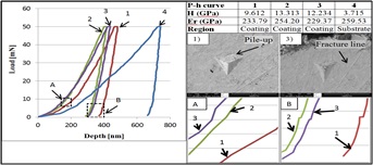
Statement of the Problem: Nanoindentation of WC-12Co thermal spray coatings has been used to evaluate the elastic modulus and hardness of coating on the polished surface of the coatings. While there has been much progress overall, limited research has been reported on the deposition and evaluation of WC-cermet coatings. The aim of this study was to evaluate the microstructural and nanohardness characteristics of tungsten carbide-cobalt (WC-Co) cermet coatings deposited by liquid suspension spraying. Methodology: Commercially available WC-Co coating powder was milled and water based suspension was produced as feedstock for the thermal spray coating process. Microstructural evaluations of WC-Co cermet coatings included XRD (X-Ray Diffraction) and SEM (Scanning Electron Microscopy). Post spraying nanomechanical evaluations were conducted using a Berkovich nanoindenter. Findings: Results indicated relatively higher modulus but lower hardness of suspension coatings. The load displacement curves during nanoindentation were characteristic of the complex coating microstructure showing signs of microcracking and pile-up. The load displacement (P-h) curves along with the SEM images of indents for S-HVOF (suspension high velocity oxyfuel) coating illustrated evidence of sink-in and pile-up of material around the indent contact residual impression during the nano-indentation process. There was some indication of microcracking during indentation as well.
Conclusions: A comparison of S-HVOF and conventional HVOF coatings points toward phase transformations occurring in the suspension spraying which led to nanocrystalline or amorphous phases. The elastic modulus of S-HVOF coatings was on average higher than the conventional HVOF coating. The load displacement curves show features which are consistent with the complex coating microstructure with evidence of micro-cracking and pile-up.
Krzysztof Z Sokalski
Czestochowa University of Technology, Poland
Title: Scaling a way for revealing self-similar features of materials and new applications
Time : 11:50-12:10

Biography:
Research Experience (some events): Dec 1999 – Aug 2016 Research Director, Czestochowa University of Technology, Institute of Computer Sciences Czestochowa, Poland. Oct 1994 – Sep 2002.Professor in Full, Jagiellonian University, Institute of Physics, Cracow, Poland. Visiting Scientist - Integrability of quantum systems, Universiteit Utrecht, Institute for Theoretical Physics Utrecht, Netherlands. Jul 1988 – Sep 1988 Visiting Scientist - Dynamical critical phenomena Universiteit Utrecht, Institute for Theoretical Physics. Apr 1988 – Apr 1988 Visiting Professor - Phase transitions and critical phenomena - lectures for PhD students, The Rockefeller University, New York City, United States Laboratory of Mathematical Physics. Feb 1988 – Oct 1994, Professor (Associate), Head of Soft Condensed Matter Department, Jagiellonian University, Institute of Physics, Kraków, Poland.
Abstract:
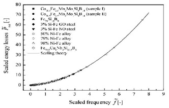
Certain features of certain materials are self-similar. This phenomenon is recognizable by scaling of measurement data corresponding to the considered self-similar feature. To perform scaling we apply notion of homogenous function in general sense. For two independent variables such a function reads P(f,B)=Bβ F(f/Bα), where P is a considered magnitude, α and β are scaling exponents, F(∙) is an arbitrary continuous function, where α, β and F(∙) have to be determined by the measurement data. Definition of P(f,B) enables us to transform all characteristics P(f,B) to the one universal function of the one variable: P(f,B)/ Bβ =F(f/Bα ). This effect is so called the data collapse and can be applied for comparison of measurement data measured in different laboratories, which enable us to estimate quality of each laboratory series. Another application of the data collapse is compression of large experimental data. If the considered data are produced by a self-similar system then one can store them in a form of continuous curve. The data collapse enables us to introduce an absolute dimensionless characteristic: 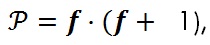
1), where P and f are dimensionless P and f, respectively. This characteristic divides { P, f } space into the two independent subspaces of materials’ characteristics.
Finally, the scaling supplemented by pseudo-equation of states plays basic role in creation of algorithms for designing of modern materials.
The presented results base on experimental data of Soft Magnetic Materials and Soft Magnetic Composites. Where, P(f,B) is density of power loss, f is frequency of the field’s modulation and B is maximum of magnetic induction. One can apply this simple mathematics to any self-similar object. However, ultimately one must say that the degree of success achieved when applying the scaling depends on the property of the data. The data must obey the scaling.
Etsuji Ohmura
Osaka University, Japan
Title: Laser assist break of hard and brittle materials
Time : 12:10-12:30

Biography:
Dr. Ohmura is a professor of Osaka University. His main field of research is intelligent laser processing systems, especially theoretical analysis and computer simulation to gain deeper understanding of the complicated physical phenomena in laser material processing, influence of laser optics, and nonlinear optical phenomena.
Abstract:
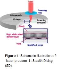
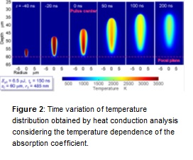
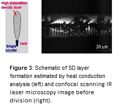
When laser beam with a high energy density is irradiated onto a material, the energy of the beam is converted into thermal energy by absorption, and the temperature rises locally. Thermal diffusion occurs due to a steep temperature gradient. However, as the thermal diffusion time and the thermal diffusion length are very short, a phase change such as fusion, evaporation, sublimation, occurs instantly because energy is added locally in a very short time. The thermal stress caused by this temperature gradient is large and as a result, hard and brittle materials that are difficult to process by mechanical processing can be processed by non-contact processing. Two examples of laser assist break of hard and brittle materials are introduced here. (1) Stealth dicing of the silicon wafer: A permeable nanosecond pulse laser is focused into the interior of a silicon wafer and scanned in the horizontal direction, causing a belt-shaped modified layer to be formed in the wafer (Fig. 1). Applying tensile stress perpendicularly to this modified-layer separates the silicon wafer very easily into individual chips. This method is called “stealth dicing (SD)”. In order to establish a more highly reliable dicing technology and investigate the optimum processing conditions, the formation mechanism of the internal modified layer was studied (Figs. 2 and 3). (2) Laser scribing of glass: Glass sheet is used for flat panel displays, and laser scribing is being used as the separation process. We conducted thermal stress analysis and crack propagation analysis in order to clarify the processing phenomena and control factor.
Ki-Soo Lim
Chungbuk National University, Korea
Title: Self-organized periodic nanostructures on the surfaces of semiconductors and dielectrics by scanning femtosecond laser pulses
Time : 12:30-12:50

Biography:
Ki-Soo Lim is a full professor of physics department at Chungbuk National University in South Korea. He has been working on laser spectroscopy of rare-earth ion doped crystals, glasses, glass-ceramics, and semiconductors. He also studied 3-D bit or holographic data storage in glass, photopolymers and photovoltaic materials. Recent interests and achievements include precipitation and optical properties of glass-ceramics containing fluoride nanocrystals, and micro-nanostructure fabrication on the surface of dielectric materials and polymers by femtosecond laser. He received his B.S. and M.S. degree in Physics at Seoul National University in 1977 and 1980 respectively. He then did his PhD in physics at University of Connecticut, USA, and worked at University of Georgia as a research associate. He joined Chungbuk National University in 1990 after working at Korea Standard Research Institute.
Abstract:
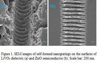
We report the self-formed nanogratings on the surfaces of semiconductors (ZnO and GaN) and dielectric materials (fused silica, borate glass, LiTaO3, LiVO3, sapphire) prepared by scanning focused femtosecond laser pulses at 800 nm with a repetition rate of 1 kHz. Laser fluence range for nanograting self-formation is very narrow. We find a series of periodic-structure orientation is perpendicular to the linear laser polarization. The period of grating structures on the dielectric surface depends on laser power and scan speed, and increases in the range of 200∼300 nm with scan speed and laser pulse energy. In contrast, GaN shows about 600 nm period in the same power range as the dielectric materials. Its period decreases to 450 nm when the laser power is reduced ten times. It also has much lower laser ablation threshold than dielectrics and ZnO, indicating characteristics of metal-like nanogratings due to its high plasma density, large thermal conductivity, and multiphoton absorption coefficients at 800nm. Emission from nanograting area of sapphire indicates the existence of oxygen vacancies. Figure 1 shows the nanograting structure formed by scanning femtosecond laser pulses at 40 μm/s speed of on the surfaces of LiVO3 and ZnO with 0.13 and 0.09 mW power respectively.
For applications, surface nanostructures can be used to improve out-coupling of light in LED. Material absorption can be also significantly enhanced due to surface nano-structures produced by fs-laser pulse processing, applicable to sensing and solar cells.
Lahcène Ouahab
CNRS, Université de Rennes 1, France
Title: Lanthanides-redox ligands for single molecule magnets and luminescence
Time : 12:50-13:10

Biography:
Lahcène Ouahab received his PhD thesis from the University of Rennes1 in 1985. He was “Maître de conférences” at the University of Constantine (Algeria) and then associate Professor at the University of Rennes1 (1988) before getting a permanent position in CNRS as “chargé de recherche” in 1989. He is presently a CNRS director of research and leads the molecular materials research group. He was director of the “Laboratoire de Chimie du Solide et Inorganique Moléculaire UMR6511-CNRS Université de Rennes1” 2004-2006. He was awarded the 1998 prize of the Coordination Chemistry Division, the 2011 Claude Berthault Prize of the “Académie des Sciences” and the 2012 “Grand Prix Pierre Süe” of the French Chemical Society. His fields of research include molecular materials, in particular, multifunctional materials, charge transfer complexes, radical ion salts, organic-inorganic hybrids, polymeric coordination complexes and polyoxometallates
Abstract:
Lanthanide-based complexes have greatly contributed to the development of molecular magnetism in the last decade and more particularly in the branch of single molecule magnets (SMMs). The main reasons are their large magnetic moments associated to their intrinsic large magnetic anisotropy. The splitting of the multiplet ground state of a single-ion in a given environment is responsible of the trapping of the magnetic moment in one direction in SMMs. However, the analyses of the crystal field effects on the magnetic anisotropy are not so common. A better understanding of the magneto-structural correlations in lanthanide-based complexes should provide tools to improve their potentialities. In this presentation we will focus on the specific magnetic properties of TTF-based lanthanide mononuclear and polynuclear complexes. We will show how optimize the SMM behavior playing on i) the modulation of the supramolecular effects via chemical modifications of the TTF ligand, ii) simple molecular engineering modifying the electronic distribution and symmetry of the coordination polyhedron, iii) magnetic dilutions (solution and doping) and iv) isotopic enrichment of the dysprosium.
Haruhiko Morito
Tohoku University, Japan
Title: rystal growth of Na-Si clathrates by the flux method
Time : 14:00-14:20

Biography:
Haruhiko Morito has his expertise in material science and engineering. The main objective of his research is to develop an emerging material which has a new function and new physical properties. In particular, he has developed new functional ceramics containing alkali metals. He has also developed a new crystal growth process based on the binary phase diagram of sodium and silicon. He has synthesized the various silicon-based materials by the sodium flux method.
Abstract:
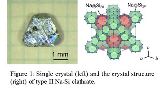
Introduction: Si clathrate compounds have been widely studied due to their unique open-framework structures of Si polyhedrons. Two types of Si clathrates encapsulating Na atoms have been known: type I (Na8Si46) and type II (NaxSi136, 0 < x ≤ 24). These Na-Si clathrates have been generally synthesized by thermal decomposition of a Na-Si binary compound, Na4Si4, at 673–823 K under high-vacuum conditions (<10−2 Pa), and the obtained samples were in the form of powder with a particle size in the micrometer range. The purpose of this study is the crystal growth of the type I and type II Na-Si clathrates by using a Na-Sn flux. Experimental: The starting material of a mixture of Na, Na4Si4, and Na15Sn4 was prepared by heating Na, Si, and Sn (molar ratio, Na/Si/Sn = 6:2:1) at 1173 K in Ar atmosphere. The mixture was heated at 673–873 K for 6–24 h in the container with a temperature gradient. After heating, air-sensitive compounds in the samples, such as Na-Sn compounds, were reacted with ethanol, and the water-soluble reactants were removed by washing with water. Sn present in the products or formed by the ethanol treatment was removed by dissolution in a dilute nitric acid aqueous solution. Results: The single crystals of type I clathrate were crystallized due to the evaporation of Na from the Na-Sn-Si solution at 673–773 K. Most of the single crystals had sizes of several hundred micrometers to 1 mm, and the maximum size reached to about 3 mm. Heating the starting mixture at 823–873 K resulted in the crystal growth of the type II clathrate. The single crystals having {111} habit planes grew up to about 2 mm in size as shown in Fig. 1.
Isaac D Adebiyi
Vaal University of Technology, South Africa
Title: Microstructure and surface properties of Ti-6Al-4V cold spray coated with SiC-based cermet
Time : 14:20-14:40

Biography:
Isaac Adebiyi is a lecturer in the Department of Metallurgical Engineering, Vaal University of Technology, Vandebijlpark, South Africa. He holds a doctoral degree in Metallurgical engineering with specialization in new materials development. His research interests include surface modification of engineering materials (Laser Materials Processing, Cold Spray Coating, High Velocity Oxy Fuel Coating etc.), Additive Manufacturing, Computational Fluid Dynamics Modelling and Simulation, Tribology and Wear Mitigation, Process Optimization, Alloy Design and Physical Metallurgy of Alloys, Microstructure and Phase Evolution Studies, Multifunctional Coatings Development, and Development of Smart and Advanced Materials. He received an award for Innovation and excellence in the use of stainless steel by the Southern African Stainless Steel Development Association. He has authored many publications and has chaired plenary section and moderated international conference.
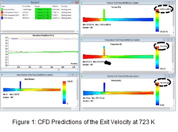
Abstract:
Statement of the Problem: A more ubiquitous application of Ti-6Al-4V in the aerospace industry has been hindered by its poor set of surface properties. The cold spray coating (CSC) process is suitable for improvements in the surface properties but the process is very complex, and highly dependent and sensitive to small changes in its many process parameters. Moreover, the CSC is also very selective of the choice of powder materials. The choice is not only based on application requirements but also on plastic deformability of the powder. Methodology & Theoretical Orientation: This investigation presents a mathematical identification of the optimum process parameters by using a constitutive equation to solve the continuity, momentum and the energy equations governing the flow of fluid through the low-pressure cold spray nozzle. A CFD analysis is performed to determine the input temperature that will yield the calculated velocity by using the meshing tool of Solidworks to analyze the distribution of velocity, temperature, and pressure in the cold spray nozzle and predict their exit values. The optimum parameters were used to deposit a SiC-based cermet on Ti-6Al-4V. The microstructure and phase evolution in the coatings were studied; porosity was measured using ImageJ analysis software; the hardness was measured using Vickers hardness tester; adhesion test was performed according to ASTM C633-1; and the dry sliding wear behaviour was studied in a ball-on-disc configuration using a load of 25 N at a frequency of 5 Hz. Findings: Results show that the initial phases in the feedstock powder were retained in the coatings. No detrimental phase transformation, decomposition and/or decarburization of the SiC. There was peak shift between the phases in the feedstock powder and that of the coatings. This is traced to impact-induced micro-straining, amorphization and grain refinement. A good adhesion strength, and improvements in hardness and wear resistance were obtained in the coated samples although with a higher coefficient of friction which is traceable to higher strength and lack of micro films in the coating. Conclusion & Significance: The improved surface properties of the coating will lengthen the lifespan of the expensive Ti-6Al-4V alloy, leading to significant cost savings for the aerospace industry.
Tengyuan Zhang
Western University, Canada
Title: Facile fabrication of hybrid copper-fiber conductive features with enhanced durability and ultra-low sheet resistance for low-cost high-performance paper-based electronics
Time : 14:40-14:55

Biography:
Tengyuan is currently a Ph.D. Candidate of Mechanical & Materials Engineering in Western University, London, Ontario. His research explores printed flexible and stretchable electronics. Based on his research, he co-founded Nectro Inc. in 2015 with the goal of developing novel nano-materials and bringing them to people’s life. Tengyuan was awarded the Vanier Canada Graduate Scholarship in 2015 and won the Doctoral Excellence Research Award in 2016. Now, he looks to combine cutting-edge nanotechnology and advanced chemical/material science to find a robust, low-cost solution for manufacturing high-performance, high-resolution flexible and stretchable electronics.
Abstract:
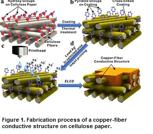
The accelerating arrival of the Internet of Things (IoT) era creates huge demand for low-cost, high-performance paper electronics. However, fabricating highly conductive circuit on low-cost cellulose paper is challenging due to its high roughness and resolution loss caused by capillary effect.
To address these challenges, we propose a scalable, cost-effective method to fabricate high-performance electronics on regular cellulose paper. Taking advantage of the unique porous structure of cellulose paper, we activate the three-dimensional electroless deposition of copper for fast generation of the hybrid copper-fiber highly conductive structure. Currently, the sheet resistance of most PE product is 50 mΩ/sq. With the technology mentioned above, 5 mΩ/sq (10 times better) can be easily achieved with low cost and high resolution (100 microns feature size). Thanks to its unique copper-fiber hybrid structure, both the physical and electrical properties are greatly enhanced for wider variety of applications. To demonstrate its promising application, a functional battery-free energy harvesting device and a high-performance planar antenna for RFID were fabricated and tested using the proposed method.
Poster Presentation @ 15:10-16:30 in Foyer
Click on Awards category for Poster Presentations

Biography:
Isaac Adebiyi is a lecturer in the Department of Metallurgical Engineering, Vaal University of Technology, Vandebijlpark, South Africa. He holds a doctoral degree in Metallurgical engineering with specialization in new materials development. His research interests include surface modification of engineering materials (Laser Materials Processing, Cold Spray Coating, High Velocity Oxy Fuel Coating etc.), Additive Manufacturing, Computational Fluid Dynamics Modelling and Simulation, Tribology and Wear Mitigation, Process Optimization, Alloy Design and Physical Metallurgy of Alloys, Microstructure and Phase Evolution Studies, Multifunctional Coatings Development, and Development of Smart and Advanced Materials. He received an award for Innovation and excellence in the use of stainless steel by the Southern African Stainless Steel Development Association. He has authored many publications and has chaired plenary section and moderated international conference.
Abstract:
Statement of the Problem: A more ubiquitous application of Ti-6Al-4V in the aerospace industry has been hindered by its poor set of surface properties. The cold spray coating (CSC) process is suitable for improvements in the surface properties but the process is very complex, and highly dependent and sensitive to small changes in its many process parameters. Moreover, the CSC is also very selective of the choice of powder materials. The choice is not only based on application requirements but also on plastic deformability of the powder. Methodology & Theoretical Orientation: This investigation presents a mathematical identification of the optimum process parameters by using a constitutive equation to solve the continuity, momentum and the energy equations governing the flow of fluid through the low-pressure cold spray nozzle. A CFD analysis is performed to determine the input temperature that will yield the calculated velocity by using the meshing tool of Solidworks to analyze the distribution of velocity, temperature, and pressure in the cold spray nozzle and predict their exit values. The optimum parameters were used to deposit a SiC-based cermet on Ti-6Al-4V. The microstructure and phase evolution in the coatings were studied; porosity was measured using ImageJ analysis software; the hardness was measured using Vickers hardness tester; adhesion test was performed according to ASTM C633-1; and the dry sliding wear behaviour was studied in a ball-on-disc configuration using a load of 25 N at a frequency of 5 Hz. Findings: Results show that the initial phases in the feedstock powder were retained in the coatings. No detrimental phase transformation, decomposition and/or decarburization of the SiC. There was peak shift between the phases in the feedstock powder and that of the coatings. This is traced to impact-induced micro-straining, amorphization and grain refinement. A good adhesion strength, and improvements in hardness and wear resistance were obtained in the coated samples although with a higher coefficient of friction which is traceable to higher strength and lack of micro films in the coating. Conclusion & Significance: The improved surface properties of the coating will lengthen the lifespan of the expensive Ti-6Al-4V alloy, leading to significant cost savings for the aerospace industry.
- Session II
Track 3: Advanced Emerging Materials
Track 5: Materials: Characterization and Applications
Location: West Minster South

Chair
Klaus G. Nickel
University Tübingen, Germany

Co-Chair
David Kennedy
National Research Council of Canada, Canada
Session Introduction
Klaus G. Nickel
University Tübingen, Germany
Title: The potential of improving building construction materials by a biomimetic approach
Time : 10:00-10:20

Biography:
Klaus G. Nickel is Professor for Applied Mineralogy at the Faculty of Science of the University of Tübingen. His career involved a Dipl-Geol. from the University of Mainz (D), a PhD from the University of Tasmania (Hobart, AUS) and research positions at Max-Planck-Institutes (for Chemistry, Mainz, and Metals Research, Stuttgart). His main research interest is in materials science in the field of advanced ceramics and composites. The research covers processing, characterisation and evaluation of technical ceramics, typically alumina and zirconia in the oxides and carbon, carbides, nitrides, borides on the non-oxide side. Particular expertise exists in the chemical property evaluation (oxidation and corrosion). Other research goals are phase relations, mechanical properties and bionics of biomaterials and ceramics.
Abstract:
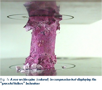
The design of spines from some reef inhabiting sea urchins (Heterocentrotus mamilatus, Phyllacanthus imperialis) has been shown to be responsible for a high energy dissipation during compressive straining. It is shown that unusually high stresses are required to compress the material, which fails in a "graceful" manner during an overall straining of several tens of percent. The principal behind the mechanism involves the layering / gradation / ordering of pore space within a basically brittle material (Calcite). We will show the details of the structures and the results of the characterization by uniaxial compression and pin indentation. The natural material has a hierarchical design including a structuring on the nano-scale to prevent a failure by simple cleavage. It would therefore be difficult to scale up all structural features of this brittle material. We will discuss how improvements of material can nonetheless be implemented by abstracting only the more macroscopic features and choosing a suitable material.
First efforts to apply this biomimetic principle to concrete as a modification of functional graded concretes confirm the effectiveness in construction materials. The design is not only beneficial for failure tolerance in cases of impacting objects but improves at the same time thermal insulation properties and lowers the total weight of constructions. The concrete was realized by spraying and slip casting methods. We will also present a recently developed alternative method for the manufacture of 3D concrete constructions (“hydroplotting”), which allows the realization of very detailed designs.
David Kennedy
National Research Council of Canada, Canada
Title: Quantifying the biological fate of nanosilver
Time : 10:20-10:40

Biography:
David Kennedy is an expert in biological inorganic chemistry with nearly a decade of experience working at the nano-bio interface. He currently works in the areas of nano- and bio-metrology at the National Research Council Canada. Previously, David has also held posts in chemical biology, molecular imaging and nanomedicine both at the NRC and MPI in Berlin, Germany. Currently David is focused on building new tools for standardizing measurements of nanomaterials in biological systems. This also includes the use of new nanobiomaterials used to mimic living tissues. Research in David’s lab also partners across several other government organizations including Health Canada, Environment Canada and the Canadian Food Inspection Agency, as well as several different parts of the NRC.
Abstract:
With a growing number of high precision tools for studying biological systems, it is important to develop traceable quantitative methods that result in accurate measurements. Because biological systems are both complex and fluxional, context is vitally important for such measurements in order for them to be accurate. Correlation of measurements through space and time can provide such quantitative assessments. Metallic nanoparticles pose many challenges for measurement in cellular systems. The metal can interfere with the detection method and the particles can change in size and shape over time and in association with different biological molecules.
At the National Research Council we seek to correlate detailed physical characterization of silver nanoparticles with biological measurements to generate methods for measuring the impact of nanosilver on different cell types and quantifying the specific interactions of nanosilver with biological molecules. Correlating changes in nanoparticles over time in biological fluids helps to provide an understanding of nanoparticle behaviour and results in higher reproducibility of observed biological endpoints. Surface coatings play a pivotal role in recognition of the particles by cellular receptors suggesting active transport plays a critical role in the nanosilver life cycle.
Physical and chemical differences between silver nanoparticles and changes that occur in biological test media can be correlated to toxicity, and different mechanisms for toxicity are apparent. Uptake rates and localization is also different between different cell lines. Uptake and localization of particles provides evidence that nanosilver should not be treated as a single material but should be studied as an array of materials with different properties in different biological systems.
Yutaka Wakayama
National Institute for Materials Science (NIMS), Japan
Title: Photochromic organic field-effect transistors: Molecules, device properties and laser patterning of circuits
Time : 11:00-11:20

Biography:
Yutaka Wakayama served at Asahi Glass Company, as a research engineer from 1989 to 1994. He was a research staff member at Tanaka Solid Junction Project, ERATO, JST from 1994 to 1998, and received his Ph. D degrees from University of Tsukuba in 1998. After working as a postdoctoral fellow at Max-Planck Institute for Microstructure Physic, Germany in 1998-1999, he joined National Institute for Materials Science (NIMS) in 1999. Now, he belongs to International Center for Materials Nanoarchitectonics (WPI-MANA) of NIMS. His current research interests are self- and directed-assemblies of molecules, functional organic field-effect transistors and molecular nanoelectronics.
Abstract:
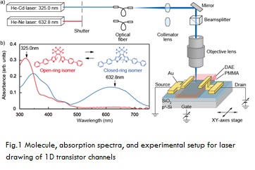
We developed an optically controllable organic field transistor (OFET) by employing photochromic diarylethene (DAE) molecules as a transistor channel layer. DAE molecules are known to undergo photochromic reaction, i.e., reversible conformational change between closed- and open-ring isomers by alternating ultraviolet (UV) and visible (VIS) light irradiation. We found that the drain current in the DAE-based OFET also showed reversible change accompanied by this conformational change; the closed-ring isomer produced by UV light exhibited a transistor operation under appropriate gate and drain bias voltages, meanwhile the open-ring isomer produced by VIS light showed no drain current. As a result, a remarkably high on/off ratio of 1,000 was achieved. The drain current modulation can be attributed to the drastic transformation in the π-conjugation system in association with the photo-isomerization. These results present two important messages. The first one is that this compound has dual properties: organic semiconductor and photochromism. The second is that a phase transition between semiconductor and insulator can be induced by light irradiation.
Based on these achievements, we demonstrate laser drawing of one-dimensional (1D) channels on an OFET with a photochromic DAE layer (See Fig.1). The main findings are: i) a number of 1D channels can be written and erased repeatedly in the DAE layer by scanning UV and VIS focused laser spots alternately between the source and drain electrodes, ii) the conductivity of the 1D channel can be controlled by the illumination conditions, and iii) it is possible to draw an analogue adder circuit by optically writing 1D channels so as to overlap a portion of the channels and perform optical summing operations by local laser illumination on the respective channels. These findings will open new possibilities of various optically reconfigurable low-dimensional organic transistor circuits, which are not possible with conventional thin film OFETs.
Md.Shafiul Azam
Bangladesh University of Engineering and Technology, Bangladesh
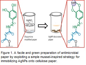
Title: A bioinspired strategy for immobilizing silver nanoparticles towards the synthesis of antimicrobial paper
Time : 11:20-11:40

Biography:
Dr. Azam is the principal investigator of a materials and surface chemistry research group in the department of chemistry at Bangladesh University of Engineering and Technology (BUET), Dhaka, Bangladesh. His multidisciplinary research is focused on the development of new multifunctional materials for energy, health and environment. Multicomponent hybrid materials for achieving increased complexity and functionality in nanoparticles have attracted enormous attention from researchers. These nanomaterials are composed of discrete domains of different components and thus can exhibit the properties of different components in the same assembly. In the Azam group, they synthesize surface-tailored, size-controlled inorganic nanoparticles and polymeric materials as well as investigate their properties and potential applications.
Abstract:
Lay Shoko
Vaal University of Technology, South Africa
Title: Effects of the chemical composition of coal tar pitch on the baking zone temperature in Soderberg electrode systems
Time : 11:40-12:00

Biography:
Lay Shoko completed his Ph.D majoring in Chemistry from North West University (South Africa) in 2014. He is currently working as a Senior Research Technologist in the Department of Chemical Engineering at the Vaal University of Technology. His thesis was focused on the studying the effects of the chemical composition of coal tar pitch on dimensional changes during graphitization. He is currently working on a projects the involve producing activated carbon from coal tar pitch and its application in removal of phenols from waste water.
Abstract:
Coal can be converted to different chemical products through processes such destructive distillation. The destructive distillation of coal yields coke as the main product with by-products such as coal tar pitch (CTP). CTP has a wide range of applications especially in the carbon processing industries with typical applications including manufacture of anodes used in many electrochemical processes as well as Söderberg electrodes used in eletric arc furnances. This paper presents results from a study carried out to establish the baking isotherm temperature of coal tar pitch during thermal treatment. Thermomechanical analysis (TMA) was used to measure the dimensional changes which take place in pitch in the baking zone during thermal treatment. Elemental analysis, Fourier Transform Infra-Red (FT-IR) and Numclear Magnetic Resonace spectroscopy were used to evaluate the chemical composition of different raw and thermally treated coal tar pitch samples. The results from this study demonstrated that the baking isotherm temperature of coal tar pitch is the same irrespective of the chemical composition and origin of the coal tar pitch. In addition to that, the results also indicated that the coal tar pitches shrunk approximately 12% if exposed to temperatures above the baking isotherm temperature up to 1300°C.
Sang-Wook Han
Jeonbuk National University, Korea
Title: Growth, structural and electrical properties of VO2/ZnO nanostructures
Time : 12:00-12:20

Biography:
Sang-Wook Han published over 70 research papers in solid state physics, nanoscience, and nanotechnology and given over 30 invited lectures. His major research field is the micro-structural and chemical property characterizations of nanomaterials using X-ray absorption fine structure (XAFS) and nanomaterial applications including sensors, battery, and solar cells.
Abstract:
VO2 is a typical metal-insulator-transition(MIT) material with the bandgap of ~0.7 eV and the Tc of ~ 70oC. VO2 is transparent and dark below and above the Tc, so that it can be applicable for smart windows by controlling the temperature. VO2 nanoparticles in a metallic phase block and scatter sunlight. The scattered sunlight by VO2 nanoparticles can be used in solar cells. We examined the local structural and electrical properties from VO2/ ZnO nanostructures by using the simultaneous measurements of x-ray absorption fine structure(XAFS) and resistance. The structural and electrical properties of VO2 depend on the length of ZnO nanorods underneath VO2. Direct comparison of simultaneously-measured resistance and XAFS from the VO2 demonstrates that the transitions of structures, local density of the V 3d orbital states, and resistance occurred in sequence during heating, whereas the properties changed simultaneously during cooling. XAFS reveals a substantial increase of Debye-Waller factors, particularly, V-V pairs along the {111} direction in the metallic phase. XAFS results indicate that soft phonon above Tc plays a critical role in the collapse of a small band gap of VO2. The local structural and the electrical properties of VO2/ZnO nanorods are considerably sensitive to the interface of VO2/ZnO as well as the length of ZnO nanorods. The interface properties of VO2 hetero-structures of should be taken into account for its applications to smart windows and solar cells.
Bi-Hsuan Lin
National Synchrotron Radiation Research Center, Taiwan
Title: Temperatureâ€dependent hard Xâ€ray excited optical luminescence to study the optical properties of the ZnO microwires
Time : 12:20-12:40

Biography:
Bi-Hsuan Lin has completed his Ph.D. from Department of Photonics and Institute of Electro-Optical Engineering, National Chiao Tung University, Hsinchu, Taiwan and postdoctoral studies from European Synchrotron Radiation Facility (ESRF) for one year. Now He works at National Synchrotron Radiation Research Center as the assistant research scientist. He is participating the construction and commission of the X-ray nanoprobe beamlime at Taiwan Photo Source (TPS), and is responsible for development of the XEOL and TR-XEOL.
Abstract:
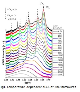
The advantages of using synchrotron radiation as the excitation source are that the tunable X-ray energy allows the preferential excitation of the elements through the X-ray absorption edges, and a suitable time structure of the synchrotron can be used to study the dynamics of luminescence of the materials. We develop the synchrotron based hard X-ray excited optical luminescence (XEOL) and time-resolved X-ray excited optical luminescence (TR-XEOL) at the X-ray Nanoprobe (XNP) facility at Taiwan Photon Source (TPS). In parallel to the construction of the XNP endstation, demonstrative XEOL experiments were conducted by unfocused X-ray beam at Taiwan Light Source (TLS). The low temperature (4.2K) and temperature-dependent XEOL with X-ray excited energy below, at and above the Zn K-edge (9.659keV) were used to obtain the further information of the optical mechanisms of the ZnO microwires. The temperature-dependent XEOL behavior of the ZnO microwires with X-ray energy at 9.67 keV was shown in Figure 1. The free A excitons, donor bound excitons and their phonon replicas can be seen unambiguously at low temperatures. The design of the XEOL and TR-XEOL at XNP and the demonstrative experimental results will be reported.
Lunch Break 13:10 onwards… @ Fraser
- Workshop
Location: West Minster South
Session Introduction
Youssef Belmabkhout
KAUST, Saudi Arabia
Title: Emerging nano-porous metal-organic frameworks materials for applications related to energy efficiency and environmental sustainability
Time : 11:55-12:40

Biography:
Dr Youssef Belmabkhout has a PhD in applied Science from the University of Mons in Belgium. He hold also a chemical engineering degree (oil and gas technologies) from the “Gubkine” Russian State University of oil and gas in Moscow (Russia). Prior to his appointment as a research scientist at the King Abdullah university of Science and technology (KAUST, KSA) in Prof Eddaoudi group, Dr Youssef Belmabkhout spent few months in ICPET-NRC (Ottawa, Canada) in 2010 working on Solid Oxide Fuel Cell. He occupied a research associate position in the department of chemistry at the university of Ottawa (Canada) with Prof Sayari from 2007 to 2010 and one and half year in the prestigious French Institute of Petroleum (IFP) in Lyon, France from 2006 to 2007. During his short research career, Dr Youssef Belmabkhout explored the use of several classes of materials for applications related to energy efficiency and environmental sustainability.
Abstract:
The Molecular Building Block (MBB) approach is a powerful strategy that permits the fabrication of tailored MOF materials for specific applications. The key factors for development of advanced new materials is the deep understanding of their structural-chemical properties in relationship with their properties in real applications.
In my talk I will illustrate the power of MBB in the development of tunable platforms with a variety of interesting properties. The perfect structural control at the molecular level of these particular platforms led to the discovery of advanced materials with potential for many gas/vapor separations such as gas storage, H2S removal, paraffin-branched paraffin separation and air conditioning. In particular, I will discuss the structural properties of separation agents, from the family of MOFs with relation to the CO2 capture capabilities from ppm level to high concentrations. These properties have direct and/or indirect relation with other attributes such as type of pore (channels, cavities or combination of both), pore size, and energetics…etc. One of the crucial parameter, is the uniformity of suitable adsorption sites over a wide range of CO2 adsorption loading. Uniform and enough strong CO2 interaction (adsorption energy level) distribution is one of the strict requirements to ensure maintaining high selectivity over a broad range of CO2 adsorption loading. This uniform high charge density in addition to narrow pore size (close to CO2 molecular size) led to unveil, for the first time, a model of MOF adsorbent with a combined mechanism involving optimal thermodynamics (energetics) and kinetics for CO2 capture at intermediate, low5 and traces6 CO2 concentration. This unique combination of high and uniform charge density and optimal pore size allowed to push the boundaries of CO2 energetics to the upper limit of physical reversible adsorption (45-60 kJ/mol) combined with highly favorable CO2 adsorption kinetics.
- Session I
Track 2: Materials and Devices
Track 4: Nanotechnology & Emerging Technologies
Location: West Minster South

Chair
Anton Liopo
The University of Texas MD Anderson Cancer Center, USA

Co-Chair
Jingyang Wang
Chinese Academy of Sciences, China
Session Introduction
Anton Liopo
The University of Texas MD Anderson Cancer Center, USA
Title: Gold-based emerging nanomaterials for imaging and experimental cancer therapy
Time : 12:40-13:00

Biography:
Anton Liopo earned his PhD degree from the Institute of Physiology the National Academy of Science (NAS) of Belarus. He later went on to join the Institute of Biochemistry of NAS of Belarus as Senior Scientist, Associate Professor, and eventually the Director of Government Program. After moving to the United States, Dr. Liopo obtained trainings in molecular biology in Department Internal Medicine and nanotechnology in Center for Biomedical Engineering at the University of Texas, Medical Branch at Galveston. He was invited and many years worked in TomoWave Laboratories Inc., where he was Lead Scientist for nanobiotechnology program. Now Dr. Liopo continues his investigations in Center for Radiation Oncology Research, UT MD Anderson Cancer Center, where he is aiming on novel nanocomposites for enhancement of cancer radio-therapy and he is also a visiting scientist in Department of Chemistry of Rice University. Dr. Liopo is a regular reviewer and member of several editorial boards of scientific journals. Dr. Liopo has more than 75 peer-reviewed publications, including monograph, book chapters and patents.
Abstract:
Gold nanoparticles of different shape and size have been designed and applied as contrast-enhancing agents for various imaging techniques: optical coherence tomography, fluorescence imaging, optical microscopy, photoacoustic imaging and sensing; and recently, for experimental cancer therapy as enhancers of thermal and radiation modes. In the current presentation, we are focusing on different sides of gold nanorods (GNRs) applications, as well as their synthesis, functionalization, and specific targeting. The role of GNRs in comprehensive cancer diagnostics and treatment was analyzed. We have created the novel GNRs’ modifications of wide-ranging aspects ratio and size with high yield and quality. The GNRs were assessed by their toxicity for altered categories, such as amount of gold, surface area, optical density of their solutions and number of particles. GNRs have been reviewed as contrast agents with near-infrared absorption as highly efficient transformers of light energy into heat. Here we present the use of GNRs as plasmonic nanoparticles for selective photothermal therapy of human acute and chronicle leukemia cells using a near-infrared laser. We have investigated GNRs as potential enhancers of radiotherapy. We have demonstrated high impact of external surface chemistry, role of molecules size and thickness of surfactant layer for damage of cancer cells by electromagnetic radiation. GNRs were evaluated as theranostic agents for imaging, photothermal and radiation modalities. The results may impact pre-clinical GNRs’ applications, molecular imaging, and quantitative sensing of biological analytes.
Jingyang Wang
Chinese Academy of Sciences, China
Title: Strategic modification of nanostability for super thermal insulating materials
Time : 13:00-13:20

Biography:
Dr. Jingyang Wang is the distinguished professor and division head in the High-performance Ceramics Division at the Shenyang National Laboratory for Materials Science, China. He has been internaitonally recognized for his sustained contributions to innovative technology in processing bulk, low-dimensional and porous ceramics, and to fundimental understanding of multi-scale structure-property relationship of advanced structural ceramics. His works have extensively covered fundemental and technological developments of carbides, nitrides, oxynitrides, silicates, and hafnates for extreme environment applications. He has published 185 peer-reviewed SCI papers (WoS H-index factor 38), hold 18 registered patents, and has delivered more than 50 keynote/invited lectures. Dr. Wang was the recipient of Acta Materialia Silver Medal (2016) and National Leading Talent of Young and Middle-aged Scientists (China, 2015), and served as the Chair-elect (2016) of Engineering Ceramic Division of The American Ceramic Society (ACerS) and the program chair of 41st ICACC hosted by ACerS in Florida.
Abstract:
The critical challenge of current nanoscale oxide super thermal insulation materials, such as SiO2 and Al2O3 nano-particle aggregates and their composites, is the critical trade-off between extremely low thermal conductivity and unsatisfied thermal stability (nanostability typically below 1100oC). It is crucial important to modify current materials and further discover novel candidates which could balance the two key properties. This presentation shows progresses on optimal thermal stability of modified Al2O3 nano-paticle aggregate; and in addition, new candidates of super thermal insulation materials, such as nano-Si3N4 and nano-SiC, which are commonly believed as excellent heat conductors. Especially, the new nano-systems exhibited good nanostability up to 1500°C. The striking results incorporated superior sintering stability of structural ceramics as SiC and Si3N4 with multiple phonon scattering mechanisms in nano-materials. It is possible to put forward this novel concept to design and search new types of high temperature thermal insulation materials through nano-scale morphology engineering of structural ceramics with excellent thermal stability, regardless their high intrinsic lattice thermal conductivities.
Moon-Ho Ham
Gwangju Institute of Science and Technology, Republic of Korea
Title: Engineering graphene and TMDCs for nanoelectronic device applications
Time : 14:00-14:20

Biography:
Dr. Moon-Ho Ham is an associate professor in the department of Materials Science and Engineering at Gwangju Institute of Science and Technology (GIST), South Korea. Professor Ham received his B.S. and Ph.D. degrees in Materials Science and Engineering at Yonsei University, South Korea. He was a postdoctoral associate in Chemical Engineering at Massachusetts Institute of Technology. His research focuses on nanomaterials including nanocarbon and 2D materials for nanoelectronic and energy applications.
Abstract:
Two-dimensional (2D) materials such as graphene and transition metal dichacogenides (TMDCs) have unique physical and electrical properties. There is currently interest in taking advantage of these properties for future electronic applications. In this talk, I first introduce a modified chemical vapor deposition (CVD) technique for the production of large-area, high-quality continuous monolayer graphene films from benzene on Cu at 100–300 °C at ambient pressure. In this method, we extended the graphene growth step in the absence of residual oxidizing species by introducing pumping and purging cycles prior to growth. Further, Cu/graphene stacked interconnects are fabricated by directly synthesizing graphene onto Cu interconnects using this method, which show the improved electrical properties compared to Cu interconnects. In the second part, I present a simple and facile route to reversible and controllable modulation of the electrical and optical properties of WS2 and MoS2 via hydrazine doping and sulfur annealing. Hydrazine treatment of TMDSs improves the field-effect mobilities and photoresponsivities of the devices. These changes are fully recovered via sulfur annealing. This may enable the fabrication of 2D electronic and optoelectronic devices with improved performance.
Ken Bosnick
National Research Council Canada, Canada
Title: Nanocarbon composites for mechanical and barrier applications
Time : 14:20-14:40

Biography:
Dr. Ken Bosnick is a Research Officer with the National Research Council (NRC) at the National Institute for Nanotechnology (NINT) in Edmonton, Canada. He is currently leading or contributing to a number of projects involving nanocomposites. He is leading a large cross-NRC collaborative project through NINT aimed at producing high-performing barrier films, such as for food packaging and anti-corrosion coating applications, by processing graphenic and cellulosic nanomaterials with polymers. He is also leading a smaller project at NINT concerned with producing smart materials capable of sensing meat spoilage. For the Security Materials Technology Program, he is developing new carbon nanotube / ceramic hybrids for processing into ceramic composites for armour applications, including conformal metallic catalyst deposition by atomic layer and chemical vapor techniques.
Abstract:
Nanoscale allotropes of carbon, including carbon nanotubes (CNTs) and graphene nanoplatelets (GNPs), show a great deal of promise as functional fillers in nanocomposite materials. The extreme linear aspect ratios, strong sp2 carbon bonds, and high chemical stability all contribute to making CNTs ideal reinforcement fillers for mechanical applications. Conversely, the high aspect ratio planar nature of graphene and GNPs, along with their high impermeabilities, suggest applications as barrier materials. In this talk, we discuss our work on CNT – aluminum oxide (AO) composites for mechanical applications, including as ballistic armour, and GNP – polymer composites for high barrier applications, including oxygen barriers for food packaging and anti-corrosion coatings. CNT – AO hybrid structures are produced by depositing CNTs as conformal coatings on various AO materials, including powders and fabrics (see Figure 1(a)). The deposition is carried out in a large-volume chemical vapor deposition reactor, following a conformal catalyst deposition from solution or via an atomic layer deposition process. The CNT – AO hybrids are sintered into composite materials under high pressure and characterized for mechanical enhancements. Increases in fracture toughness of as high as 71% have been found from these CNT – AO composites. GNP materials are melt-processed with polyethylene (PE) and extruded into packaging films (see Figure 1(b)), which are characterized for their oxygen transmission rates. It is found that the GNP – PE films show comparable oxygen transmission rates to the neat PE films, indicating that further processing will be necessary to realize the desired enhancements. The GNP materials are also solution processed with epoxy (EP), cast onto steel substrates, and cured to form coatings. The efficacy of these coatings as anti-corrosion barriers is established by electrochemical and salt-fog corrosion tests. Early results suggest that the GNPs are enhancing the anti-corrosion performance of the EP films.
Dongling MA
Institut National de la Recherche Scientifiue (INRS), Canada
Title: Developing nanostructured materials for harvesting more photons
Time : 14:40-15:00

Biography:
Dongling Ma is a full professor at Institut National de la Recherche Scientifique (INRS), Canada. Her main research interest consists in the development of various nanomaterials (e.g., quantum dots, catalytic nanoparticles, plasmonic nanostructures, and different types of nanohybrids) for applications in energy, catalysis, and biomedical sectors. Before joining INRS in July 2006, she was awarded Natural Sciences and Engineering Research Council Visiting Fellowships and worked at National Research Council of Canada from 2004 to 2006. She received her Ph.D. degree from Rensselaer Polytechnic Institute (USA) in 2004.
Abstract:
Efficiently harvesting visible and near infrared (NIR) photons represents an attractive approach to improve the efficiency of solar-to-electricity conversion, solar-to-fuel conversion and photocatalysis. Plasmonic nanostructures with unique surface plasmon resonance have recently been explored for enhancing solar energy harvesting in the visible and NIR regimes. On the other hand, NIR quantum dots (QDs) with size tunable bandgaps and high potential for multiple exciton generation represent a class of promising materials for new generations of solar cells. In this talk, I will present our recent work on the synthesis of plasmonic nanostructures, NIR QDs, and related assemblies as well as their applications in solar cells, solar fuel and photocatalysis. Acknowledgement: The speaker would like to acknowledge the financial support from NSERC, FQRNT, and NanoQuebec. The presenter sincerely thanks all co-authors in the following publications
Lin Jiang
Soochow University, China
Title: Plasmon-enhanced optoelectronic devices based on metal nanostructures
Time : 15:00-15:20

Biography:
Lin Jiang received her B.Sc. and Ph.D. degree in chemistry from Jilin University, Jilin, China, in 2000 and 2005, respectively. She was awarded the Alexander von Humboldt Research Fellowship in 2006 and worked at Physical Institute of Muenster University in Germany from 2006 to 2009. Then she became a senior research fellow in 2009 at the school of materials science and engineering in Nanyang Technological University, Singapore. Currently, she is a professor at Institute of Functional Nano & Soft Materials (FUNSOM), Soochow University, China since 2012. Mainly focused on the self-assembly of novel nano-structured materials, and optoelectronic complex devices. She has Published over 50 SCI papers in high quality journals, such as Acc. Chem. Res., Adv. Mater., Energy enviyon. Sci., ACSNano, Adv. Funct. Mater., etc.
Abstract:
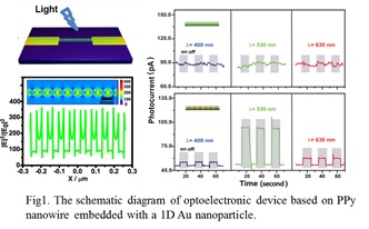
Plasmonics confine the light into nanoscale dimensions much beyond the diffraction limit by coupling the light with the surface collective oscillation of free electrons at the interface of the metal structure and the dielectric. The resonant collective oscillations give rise to an enhanced electron-magnetic field correlate with high density optical states.It modifies the light-matter interaction which results in enhanced absorption, emission or energy transfer. Hence, this photo-response mechanism makes the plasmonic structures to be an attractive study candidate to enhance the function of the optoelectronic devices, such as photodetector, solar cell, and light emitting diodes (LEDs). So far, it is still desirable to develop more unique plasmonic structures and explore their plasmon effects on devices performance to develop new-generated optoelectronic devices. Herein we introduced the research results of plasmon enhanced optoelectronic devices (photo detector, organic light emitting diode, sensors, etc.) by incorporation with different plasmonic nanostructures (zero-dimension, one-dimension or two-dimensional multiplexed plasmopnic nanostructures) and revealed the involved effective photon-management enhancement mechanism. The remarkable performance enhancement of the devices will guide the potential applications of plasmonic structures in next high-speed and high-density integrated optoelectronics and other plasmon assisted advanced devices.
Shao-Chin Tseng
National Synchrotron Radiation Research Center, Taiwan
Title: To explore nano world and material structure stress by X-ray nano probe at Taiwan photon source
Time : 15:20-15:40

Biography:
Shao-Chin Tseng has completed his PhD from department of materials science and engineering, National Taiwan University. He is the assistant scientist of National Synchrotron Radiation Research Center. He studies on Nanotechnology, X-ray nanoprobe, Optoelectronic Materials, Semiconductor Process, Biomedical Sensing. He has published more than 25 papers in reputed journals.
Abstract:
The X-ray nanoprobe (XNP) will open to all professors and researches since 2017. The XNP provides versatile X-ray-based inspection technologies, including diffraction, absorption spectroscopy, imageology, and so on. Also it will improve the analysis scale of imhomogeneous materials, tiny and diluted samples to the nanoscale. Moreover, the high- transmitted XNP can be used to inspect the “Nano World” like atomic arrangements, chemical and electronic configurations, which are widely adopted in the physics, chemistry, materials science, semiconductor devices, nanotechnologies, energy and environmental science, and earth science. Beside to the opening to the researchers, it is also important to improve the inspection and research strength of the XNP in the nanomaterials field, in order to increase the academic influence of the XNP and the Taiwan Photon Source. The primary experimental technique of XNP includes X-ray fluorescence spectroscopy (for the analysis in the depth-of-field distribution of elements), extended X-ray absorption spectroscopy (for the analysis in the electronic configuration and the atomic or molecular bonding length), excitation X-ray fluorescence spectroscopy (for the analysis in the recombination and transport of carriers), in-phase scanning X-ray imageology (the Fourier phase transform calculation can improve the space resolution down to 3nm to 5nm, and detect the stress distribution inside the nanostructures). The design XNP and the experimental applications will be reported.
Ganesh Kumar Mani
Tokai University, Japan
Title: Microneedle bio-sensor: Direct, label-free, real time detection of pH in biological cells
Time : 15:40-16:00

Biography:
Ganesh Kumar Mani is a researcher at Micro/Nano Technology Center, Tokai University, Japan. He completed his Ph.D. in Nano Sensors Lab @ Centre for Nanotechnology & Advanced Biomaterials (CeNTAB), SASTRA University, Thanjavur, India. He published over 40 research papers in reputed international journals with the cumulative impact factor over 70 with a few papers under review. He is also one of the inventors in two patents titled “Low Concentration Ammonia Vapour Sensor” & “Acetaldehyde Sensor Using ZnO Nanoplatelets”. He has also delivered several keynote lectures, organized national and international conferences in various countries. His current research interests are fabrication and development of nanostructured (Nanospheres, Nanorods, Nanowires, Nanoplatelets, Nanosheets) thin film based gas/chemical sensors for predicting food quality, developing microfluidics based solid state pH/temperature/bio-sensors for biomedical applications and developing painless microneedles for healthcare applications, etc.
Abstract:
Acid–base homeostasis and pH regulation inside the body is precisely controlled by kidney, lungs and buffer systems, because even a minor change from the normal value could severely affect many organs. Blood and Urine pH tests are common in day-to-day clinical trials without out much effort. Still, there is great demand for in vivo pH testing to understand more about body metabolism and to provide effective treatments during diagnosis. The detection of pH at the single-cell level is hoping for the great level of clinical importance for the early detection of many diseases like cancer, diabetes, etc. In this research work, we have fabricated a micro region pH sensors by series of processes like electrolytic polishing to create needle structure, deposition of electrode materials using RF magnetron sputtering for pH measurements and finally testing in various biological mediums. Working and reference electrodes were Ag/AgIO3 and Sb/Sb2O3 deposited on microneedles under optimized deposition parameters. The structural, elemental and morphological properties were analyzed using XRD, XPS, EDS and FE-SEM. The fabricated tip of the microneedle probe is around 5µm analyzed by FE-SEM which size is comparable with the biological cells. pH testing was initially begin with using fish egg and various biological cells. The obtained pH sensing results were adequate with theoretical values. Since the sensor works at micro region, the potential difference is easily disturbed by atmospheric anomalies. Hence, many steps have been taken to improve the stability of the sensor. Besides that, fabricated microneedle sensor ability is proved through in vivo testing in mice cerebrospinal fluid (CSF) and bladder. The pH sensor reported here is totally reversible and results were reproducible after several routine testing.
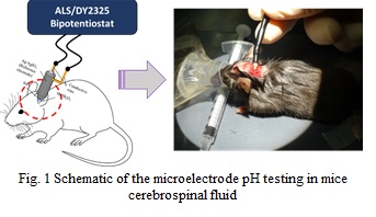
Swayamdipta Bhaduri
University of Alberta, Canada
Title: Bacteria can enhance mechanical strength of a porous medium
Time : 16:00-16:15

Biography:
Swayamdipta Bhaduri is a PhD Candidate in engineering at the Ingenuity Lab in the University of Alberta, Edmonton. He has been working on the several biological, chemical and physical aspects of the micro-scale fluid transport associated with Microbiologically Induced Calcite Precipitation (MICP) mediated by S. pasteurii. His expertise lies in the areas of nanofabrication, biomicrofluidics, and experimental fluid mechanics. He has an MS and a bachelor’s degree in Mechanical Engineering from the Indian Institute of Technology (IIT) and the National Institute of Technology (NIT) in India, respectively.
Abstract:
A class of bacterium, S. pasteurii can mediate the precipitation of calcium carbonate crystals under the right chemical environment. These crystals can actually enter a network of pores in a porous medium and cause clogging. As a result, the structure may gain significantly in strength and exhibit superior mechanical properties. This is characterized by reduction in porosity, physical pore blockage and increase in elastic moduli. This concept may be extended to a wide array of applications like underground carbon storage and repairing fractures in fragile structures. In the present study, open foam sponges of two different grades were used as porous media mimics. We performed comprehensive material testing on samples before and after bacteria treatment and drew quantitative conclusions. We tested the samples under compressive and impact loads and characterized the modification in mechanical behavior due to pore clogging. Visual observation of the actual blockage process at the pore scale was performed using Scanning Electron Microscopy (SEM) and micro-CT scans. We noticed a significant change in mechanical properties. To conclude, this particular bacterium may be used as an agent to cause pore-clogging at the microscale and the idea applied to a range of applications.
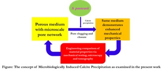
Networking & Refreshments Break 16:25-16:40 @ Tivoli’s

Biography:
Walid Tawfik, is Egyptian associate Professor, in laser spectroscopy and ultrafast lasers at the National Institute of Laser (NILES), Cairo University, Cairo, Egypt. In 1994 he joined NILES as staff member and promoted as assistant lecturer, assistant professor and associate Professor in 1996, 2000, and 2008, respectively. He received the B.SC, Master and Ph.D degrees in physics, laser physics, and laser spectroscopy in 1992, 1996, 2000, respectively, from Cairo University, Egypt. His interested in the field of ultrafast lasers and ultrafast phenomenon. He has built Fewcycle ultrafast system of 5-fs pulse duration and 0.6 mJ at 1 kHz and published 46 papers. He is a senior member of different international professional societies like IEEE, OSA, APS, and SPIE. He have collaborated with different international groups in USA, Japan, South Korea and Germany.
Abstract:
- Session II
Track 6: Biomaterials and Bioinspired Materials
Track 8: Emerging Materials for Energy Storage
Track 9: Metals and Mining
Location: West Minster South

Chair
Samuel Frimpong
Missouri University of Science and Technology, USA

Co-Chair
Aman Ullah
University of Alberta, Canada
Session Introduction
Samuel Frimpong
Missouri University of Science and Technology, USA
Title: Tire rubber material characterization for effective structural and fatigue modeling and analysis
Time : 16:40-17:00

Biography:
Frimpong is Professor and Robert H. Quenon Endowed Chair at Missouri S&T. He holds PhD (1992) from Univ. of Alberta, MS (1988) from Univ. of Zambia, and Post-Graduate Diploma (1986) and BS (1985) from KN Univ. of Science and Tech. of Ghana. His research areas include machine dynamics, machine and whole-body vibrations, fatigue modeling, augmented visualization, formation excavation, intelligent mining systems, and mine safety, health and hazards engineering. He has and continues to lead research initiatives in these areas with over $34 million funding. His research results include over 30 PhD and MS graduates, 1 book, 3 book chapters, over 200 refereed journal and conference papers and over 200 presentations. Frimpong has been recognized with Missouri S&T Chancellor’s Leadership Award, Robert Quenon Endowed Chair, Canadian Petroleum Institute’s Distinguished Lecturer Award, Award of Distinction by World Mining Congress, University of Alberta/CIDA PhD Scholar, Life Patron of UMaT Alumni Association, Grand Award by NW Mining Association and a UNESCO Research Fellowship. He is a member of the APLU Board on Natural Resources, Vice Chair of the Minerals and Energy Resources Division of NASULGC, and a member of the College of Reviewers for Canada Foundation for Innovation and Canada Research Chairs Program and ASCE-UNESCO Scientific Committee on Emerging Energy Technologies (ASCE-UNESCO SCEET). He served 5 years as a member of CDC-NIOSH Research Advisory Board, 4 years as co-chair of ASCE-UNESCO SCEET and 2 years on Japan’s Global Warming Research Consortium. He is currently the Editor-In-Chief of the Journal of Powder Metallurgy and Mining and Editorial Board Member for the International Journal of Mining, Reclamation and Environment. He is a Registered Professional Engineer and a member of the Canadian Institute of Mining, Metallurgy and Petroleum, American Society for Mining, Metallurgy and Exploration, American Society of Civil Engineers, and the Society for Modeling and Simulation International.
Abstract:
Rubber, in its natural state, has the consistency of a heavy viscous fluid with little to no use in structural applications. However, when vulcanized with sulfur, particulate fillers, silica and other strength inducing ingredients, cross-links are formed and the highly amorphous state of the rubber is transformed into an elastic solid. Thus, vulcanized rubber, in the absence of cords, is a nanocomposite. While added fillers give rubber enhanced performance characteristics (stiffness and toughness properties), their presence influence the dynamic and damping behavior of rubber in a very complex and disproportionate fashion. Numerical modeling of rubber behavior for predictive analysis remains a formidable challenge amidst successes achieved thus far. The object of this paper is to implement existing rubber material constitutive models in characterizing tensile strength and fatigue test data of rubber specimens extracted from an off-road mining truck tire. Specifically, the paper highlights modeling strategies for rubber strain softening, nonlinear viscoelasticity, strain-induced crystallization, and fatigue crack growth rate using spreadsheets, and commercially available material calibration codes. The novelty of the study lies in the calibration approach adopted for the fatigue characterization of the experimental data. An example problem to show how the characterized materials are used in a finite element analysis of a model tire is provided. The results obtained indicate enhanced durability in strain-crystallizing elastomers
Aman Ullah
University of Alberta, Canada
Title: Rapid conversion of lipids into biopolymers and conjugates
Time : 17:00-17:20

Biography:
Dr. Aman Ullah received his PhD (with distinction) in Chemical Sciences and Technologies in 2010 at the University of Genova, Italy by working together at Southern Methodist University, USA. He is currently working as an Assistant Professor at the Department of Agricultural, Food and Nutritional Science, University of Alberta. He has published more than 25 papers in reputed journals and 3 patents/patent applications. Aman was named a Canadian Rising Star in Global Health by Grand Challenges Canada.
Abstract:
Solvent free conversion of canola oil and fatty acid methyl esters (FAME's) derived from canola oil and waste cooking oil under microwave irradiation demonstrated dramatically enhanced rates. The microwave-assisted reactions lead to the most valuable terminal olefins with enhanced yields, purities and dramatic shortening of reaction times. Various monomers/chemicals were prepared in high yield in very short time. The complete conversions were observed at temperatures as low as 50 ºC within less than five minutes. The products were characterized by GC-MS, GC-FID and NMR. The prepared monomers were further converted into biopolymer and characterized in detail. In another approach, amphiphilic ABA type PEG-Lipid conjugated macromolecules have been synthesized using the copper-catalyzed azide-alkyne cycloaddition commonly termed as “click chemistry. Characterization of the conjugates has been carried out with the help of 1H-NMR, FTIR and GPC. The conjugates were evaluated for the encapsulation and release of an anticonvulsant drug (carbamazepine) as a hydrophobic drug model in the study. The micellization, drug encapsulation and release behavior of macromolecules was investigated by dynamic light scattering (DLS), transmission electron microscope (TEM) and fluorescence spectroscopy. From the results, it has been concluded that the nanoparticles had different average sizes due to different ratio of hydrophilic contents in the conjugate backbone. The Amphiphilic particle size and structure could be altered by changing the ratio of hydrophilic and hydrophobic contents. The in vitro drug encapsulations highlighted that all the drug-loaded micelles had spherical or near-spherical morphology. In vitro drug release study showed the controlled release of hydrophobic drug over a period of 50 hours. The results indicate that there is great potential of renewable lipid-based micelle nanoparticles to be used as hydrophobic drug carriers.
Deok-Won Lee
Kyung-Hee University, South Korea
Title: Hydroxyapatite–heparin–BMP-2 on modified titanium surfaces enhances the efficacy of bone formation and osseointegration: In vitro & in vivo study
Time : 17:20-17:40

Biography:
Deok-Won Lee is an oral and maxillofacial surgery specialist and associate professor of Kyung Hee University School of Dentistry. His expertise is in treating and improving the oral and maxillofacial health and wellbeing of people. His research on dental implant materials creates new pathways for improving healthcare. He is continually building and investigating on adequate material for implantation through invivo and invitro models based on years of experience in research, evaluation, teaching and administration both in hospital and education institutions.
Abstract:
Introduction: In the present study, surface-modified Ti samples with hydroxyapatite (HAp) and heparin (Hep)–bone morphogenetic protein-2 (BMP-2) complex (Ti/HAp/Hep/BMP-2) were prepared and the effects of the samples on the enhancement of bone formation and osseointegration in vitro and in vivo were investigated, as compared to Ti/HAp and Ti/Hep/BMP-2.
Method and materials: Surface-modified titanium (Ti) samples with hydroxyapatite (HAp) and heparin (Hep)–bone morphogenetic protein-2 (BMP-2) complex (Ti/HAp/Hep/BMP-2) were prepared, and their efficacies on the enhancements of bone formation and osseointegration in vitro and in vivo were examined as compared to Ti/HAp and Ti/Hep/BMP-2. The modified surfaces were characterized by X-ray photoelectron spectroscopy (XPS), scanning electron microscopy (SEM) and contact angle goniometry.
Results: In vitro studies revealed that MG-63 human osteosarcoma cell lines grown on Ti/HAp/Hep/BMP-2 increased the amounts of alkaline phosphatase (ALP) activity, calcium deposition and the levels of OCN mRNA gene expression as compared to those grown on Ti/HAp, Ti/Hep/BMP-2 or pristine Ti. Moreover, Ti/HAp/Hep/BMP-2 exhibited higher bone volume (BV), bone volume/tissue volume (BV/TV), removal torque value and bone–implant contact (BIC) than Ti/HAp, Ti/Hep/BMP-2 or pristine Ti in vivo. Histological evaluations showed that many desirable features of bone remodeling existed at the interface between Ti/HAp/Hep/BMP-2 and the host bone.
Conclusion: Consequently, Ti/HAp/Hep/BMP-2 may have potential for clinical use as dental or orthopaedic implants.
This study was supported by a grant from the National Research Foundation of Korea (NRF-2014R1A1A1002630 and NRF-2016R1A2B4014600)
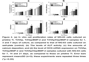
Samuel Frimpong
Missouri University of Science and Technology, USA
Title: DEM modeling of oil sands materials structures
Time : 17:40-18:00

Biography:
Frimpong is Professor and Robert H. Quenon Endowed Chair at Missouri S&T. He holds PhD (1992) from Univ. of Alberta, MS (1988) from Univ. of Zambia, and Post-Graduate Diploma (1986) and BS (1985) from KN Univ. of Science and Tech. of Ghana. His research areas include machine dynamics, machine and whole-body vibrations, fatigue modeling, augmented visualization, formation excavation, intelligent mining systems, and mine safety, health and hazards engineering. He has and continues to lead research initiatives in these areas with over $34 million funding. His research results include over 30 PhD and MS graduates, 1 book, 3 book chapters, over 200 refereed journal and conference papers and over 200 presentations. Frimpong has been recognized with Missouri S&T Chancellor’s Leadership Award, Robert Quenon Endowed Chair, Canadian Petroleum Institute’s Distinguished Lecturer Award, Award of Distinction by World Mining Congress, University of Alberta/CIDA PhD Scholar, Life Patron of UMaT Alumni Association, Grand Award by NW Mining Association and a UNESCO Research Fellowship. He is a member of the APLU Board on Natural Resources, Vice Chair of the Minerals and Energy Resources Division of NASULGC, and a member of the College of Reviewers for Canada Foundation for Innovation and Canada Research Chairs Program and ASCE-UNESCO Scientific Committee on Emerging Energy Technologies (ASCE-UNESCO SCEET). He served 5 years as a member of CDC-NIOSH Research Advisory Board, 4 years as co-chair of ASCE-UNESCO SCEET and 2 years on Japan’s Global Warming Research Consortium. He is currently the Editor-In-Chief of the Journal of Powder Metallurgy and Mining and Editorial Board Member for the International Journal of Mining, Reclamation and Environment. He is a Registered Professional Engineer and a member of the Canadian Institute of Mining, Metallurgy and Petroleum, American Society for Mining, Metallurgy and Exploration, American Society of Civil Engineers, and the Society for Modeling and Simulation International.
Abstract:
Oil sands are composite materials whose two dominant physical characteristics are the quartzose mineralogy and the large quantities of interstitial bitumen. The void spaces are also filled with a thin continuous net of water around the quartz grains with the remaining space occupied by dissolved gasses. An examination of thin sections and electron scanning micrographs reveals a typical particulate system whose mechanical behavior can be modeled based on particle interactions (contacts) at the microscale. The oil sands formation exhibits mainly a dense, interpenetrative, uncemented structure with a large number of contacts per grain. Additionally, oil sand undergoes high dilation under low normal stresses. In this paper, the microstructural and micromechanical behavior of oil sands materials is studied and an appropriate and comprehensive contact model is identified to describe its nonlinear, anisotropic and time-dependent behavior. A 2-D discrete element method (DEM) is developed to model the oil sands structures using DEM software package, Particle Flow Code (PFC2D). The time-dependent behavior of the bitumen (consisting of bonded fine particles) is represented by a Burger’s model. The quartz grains are modeled with irregular (subrounded and subangular) shape clumps (a rigid collection of disc bonded together). The thin-film of water surrounding the quartz grains is represented as a liquid bridge to determine the capillary force at the interface. The micromechanical model of the oil sand was developed with three different constitutive laws (force-displacement contact models) to represent the contact interactions of the constituents at the microscale. The paper provides theoretical foundations for understanding machine-ground interactions during excavation and for material behavior predictions. Understanding the microscopic behavior of oil sands materials would enhance long-term equipment design improvements and provide production engineers with higher equipment longevity and reliability for mine production and maintenance planning purpose.
Deok-Won Lee
Kyung-Hee University, South Korea
Title: Modifying titanium surfaces with nano-sized hydroxyapatite and simvastatin can enhance bone formation and osseointegration
Time : 18:00-18:20

Biography:
Deok-Won Lee is an oral and maxillofacial surgery specialist and associate professor of Kyung Hee University Schoole of Dentistry. His expertise is in treating and improving the oral and maxillofacial health and wellbeing of people. His research on dental implant materials creates new pathways for improving healthcare. He is continually building and investigating on adequate material for implantation through invivo and invitro models based on years of experience in research, evaluation, teaching and administration both in hospital and education institutions.
Abstract:
Introduction: The aim of the present study was to evaluate whether coating pristine titanium (Ti) with nano-sized hydroxyapatite (HAp) and simvastatin could enhance bone formation and osseointegration in vitro and in vivo because both HAp and simvastatin have the characteristic of osteogenetic induction.
Method and materials: Pristine Ti was sequentially surface-treated with NaOH,1,1-carbonyldiimidazole (CDI), beta-cyclodextrin-immobilized HAp powders (_-CD/HAp), and simvastatin before analysis using scanning electron microscopy (SEM), X-ray photoelectron microscopy (XPS), and static contact angle measurement.
Results: Simvastatin was released continually for up 28 days. Modification of the Ti surface with nano-sized HAp and simvastatin (Ti/_-CD/HAp/Sim) discs enhanced the osteogenic differentiation of MC3T3-E1 cells in vitro. Furthermore, Ti/_-CD/HAp/Sim of screw type enhanced bone formation between the screw and the host bone when the screw implanted to the proximal tibia and femoral head of rabbits.
Conclusion: These results suggest that surface modification of nano-sized HAp and simvastatin are effective tools for developing attractive dental implants.
This study was supported by a grant from the National Research Foundation of Korea (NRF-2014R1A1A1002630 and NRF-2016R1A2B4014600)
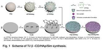
Zhihao Yue
Nanchang University, P.R. China
Title: Nano-Si: With good performance in solar cells and lithium ion batteries
Time : 18:20-18:40

Biography:
Zhihao Yue has his expertise in using nano-silicon structures to improve the efficiency of silicon solar cell and the electrochemical properties of silicon anode materials in Lithium ion batteries. He used cheaper metal nickel (compared with silver) as assisted metal to fabricate nanostructures on silicon surface and investigated its etching mechanism deeply, which is the first study about nickel-assisted chemical etching method for black silicon solar cells. Besides, he systematacially studied the effect of intrinsic electrical resistivity of silicon materials on its performance in lithium ion batteries for the first time and found that silicon materials with lower electrical resistivity present better charge-discharge properties.
Abstract:
We have done much work about silicon (Si) in solar cells and lithium ion batteries (LIBs). In the aspect of solar cell, we used silver (Ag) -assisted chemical etching method to fabricate black silicon solar cells with efficiency over 18% in 2013 and large-scale production was carried out. Besides, nickel, which is cheaper than Ag, was used as assisted metal to fabricate black silicon structure for the first time and surface reflectance of 1.59% was obtained. In the aspect of LIBs, we used Si powders made from broken Si wafers with different electrical resistivity in semiconductor industry as anode material in LIBs. We found that Si powders made from Si wafers with lower electrical resistivity show better electrochemical performance (higher capacity, and better rate performance) in LIBs. Therefore, broken Si wafers in semiconductor industry should be classified according to their electrical resistivity, which can be convenient for being used as anode raw materials for LIBs.
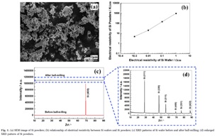
Location: West Minster South

Chair
Anton Liopo
The University of Texas MD Anderson Cancer Center, USA

Co-Chair
Jingyang Wang
Chinese Academy of Sciences, China
Session Introduction
Youssef Belmabkhout
KAUST, Saudi Arabia
Title: Emerging nano-porous metal-organic frameworks materials for applications related to energy efficiency and environmental sustainability

Biography:
Abstract:
The Molecular Building Block (MBB) approach is a powerful strategy that permits the fabrication of tailored MOF materials for specific applications. The key factors for development of advanced new materials is the deep understanding of their structural-chemical properties in relationship with their properties in real applications.
In my talk I will illustrate the power of MBB in the development of tunable platforms with a variety of interesting properties. The perfect structural control at the molecular level of these particular platforms led to the discovery of advanced materials with potential for many gas/vapor separations such as gas storage, H2S removal, paraffin-branched paraffin separation and air conditioning. In particular, I will discuss the structural properties of separation agents, from the family of MOFs with relation to the CO2 capture capabilities from ppm level to high concentrations. These properties have direct and/or indirect relation with other attributes such as type of pore (channels, cavities or combination of both), pore size, and energetics…etc. One of the crucial parameter, is the uniformity of suitable adsorption sites over a wide range of CO2 adsorption loading. Uniform and enough strong CO2 interaction (adsorption energy level) distribution is one of the strict requirements to ensure maintaining high selectivity over a broad range of CO2 adsorption loading. This uniform high charge density in addition to narrow pore size (close to CO2 molecular size) led to unveil, for the first time, a model of MOF adsorbent with a combined mechanism involving optimal thermodynamics (energetics) and kinetics for CO2 capture at intermediate, low5 and traces6 CO2 concentration. This unique combination of high and uniform charge density and optimal pore size allowed to push the boundaries of CO2 energetics to the upper limit of physical reversible adsorption (45-60 kJ/mol) combined with highly favorable CO2 adsorption kinetics.